Intel Processor Architecture Evolution: From 8080 To Pentium 4
Table of Contents
- Intel 8080 Architecture
- Intel 8086 Architecture
- Intel 80286 Architecture
- Intel 80386 Architecture
- Intel 80486 Architecture
- Intel Pentium Processor Architecture
- P6 (Intel Pentium Pro) Processor Architecture
- Intel Pentium III Processor Architecture
- Intel Pentium 4 Processor Architecture
Intel 8080 Architecture
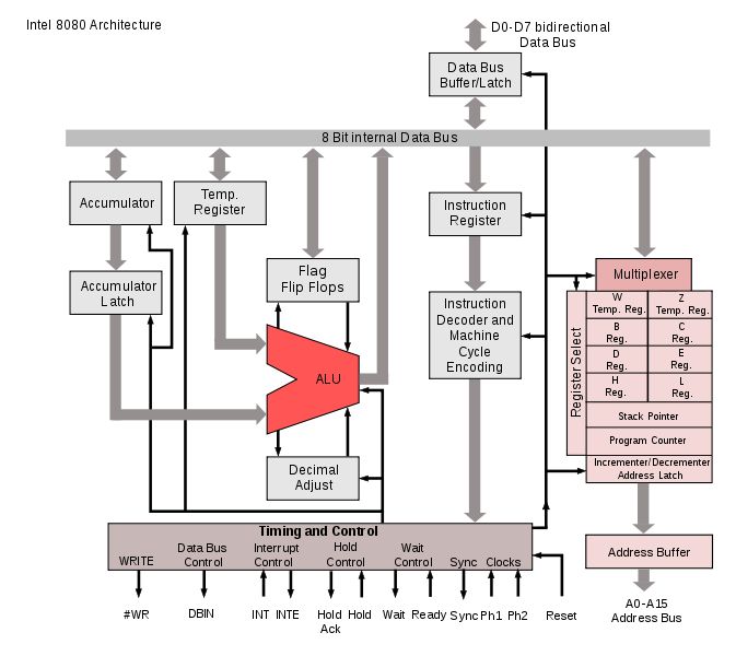
The Intel 8080 is an 8-bit microprocessor with a core architecture featuring an 8-bit internal data bus. It connects to the external environment through a bidirectional data bus (D0-D7) managed by a Data Bus Buffer/Latch.
Data Bus:
- The 8-bit bidirectional data bus allows for the transfer of data between the processor and external devices.
- Bus Buffer/Latch: Ensures stable data handling between the internal and external buses.
Processing and Control Mechanisms
The processing capabilities are powered by an Arithmetic Logic Unit (ALU), which performs arithmetic and logical operations with the help of:
ALU Support:
- Accumulator: A special register for storing intermediate results of ALU operations.
- Temporary Register: Assists in temporary data storage during operations.
- Flag Flip-Flops: Indicate conditions like zero, carry, sign, and parity after ALU operations.
- Decimal Adjust Circuit: Converts ALU results for BCD arithmetic, useful for decimal calculations.
Control and Timing:
- Control Signals: Including WRITE, DBIN for data transfer direction, and interrupt controls like INT and INTE.
- Synchronization: Sync, Ph1, and Ph2 signals coordinate the processor’s operation with external devices.
- DMA Support: The Hold/Hold Acknowledge mechanism allows other devices to control the bus for direct memory access.
- Wait/Ready Signals: Adjust processor speed to match slower memory or I/O devices.
Memory and Instruction Handling
Memory and instruction handling involve:
- Instruction Register: Stores the current instruction being processed.
- Instruction Decoder: Translates instructions into control signals for execution.
- Machine Cycle Encoding: Manages the sequence of operations for each instruction.
- Multiplexer: Routes data between various registers like the stack pointer and program counter.
- Address Buffer: Manages the 16-bit address bus, enabling access to 64K of memory.
Register Set
The register set includes:
- General-Purpose Registers: For flexible data handling.
- Stack Pointer: Manages the stack for function calls and local data storage.
- Program Counter: Keeps track of the next instruction to execute.
Intel 8086 Architecture
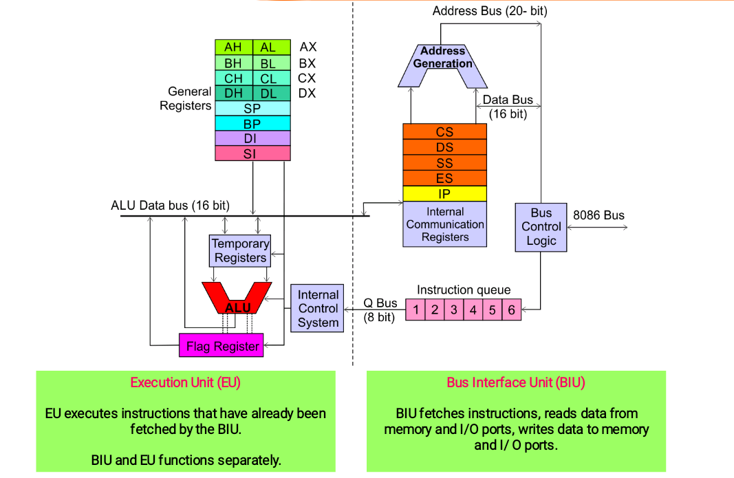
The Intel 8086 microprocessor splits its functionality into the Execution Unit (EU) and Bus Interface Unit (BIU):
General Registers:
- The EU includes four main 16-bit registers (AX, BX, CX, DX), each split into two 8-bit registers (AH/AL, BH/BL, CH/CL, DH/DL), providing flexibility for both 8-bit and 16-bit operations.
Bus Interface Unit (BIU)
The BIU manages external interactions:
- Address and Data Buses: A 20-bit address bus and 16-bit data bus facilitate communication with memory and peripherals.
- Segment Registers: CS (Code Segment), DS (Data Segment), SS (Stack Segment), and ES (Extra Segment) define memory areas for different uses.
- Instruction Pointer (IP): Tracks the next instruction in the code segment.
- Address Generation: Combines segment and offset to form physical addresses.
- Instruction Queue: A 6-byte queue prefetches instructions, enabling basic pipelining for improved performance.
Execution Unit (EU)
The EU focuses on computation:
- ALU: A 16-bit Arithmetic Logic Unit performs arithmetic and logical operations.
- Temporary Registers: Used for intermediate processing.
- Flag Register: Maintains status information like carry, zero, sign, overflow, etc.
- Independence: The EU can work on instructions from the queue while the BIU fetches new ones, enhancing efficiency.
Control and Memory Management
- Control Coordination: The Q-Bus links the EU and BIU, managing the flow of instructions and data.
- Bus Control: Logic that oversees external bus operations for data transfer.
- Memory Model: Uses a segmented approach where each segment register points to a 64KB segment within a 1MB address space.
- Segmentation: Allows for effective memory management by dividing memory into logical segments.
- Additional Registers: BP (Base Pointer), DI (Destination Index), and SI (Source Index) enhance addressing modes, making complex memory operations more efficient.
Intel 80286 Architecture
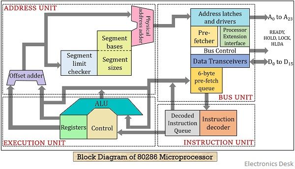
The Intel 80286 processor advances the design with three main units: the Address Unit, Execution Unit, and Instruction Unit, enhancing performance and introducing protected mode capabilities.
Address Unit and Memory Management
Memory Management:
- Segment Bases and Sizes: Define and manage memory segments for both real and protected modes.
- Segment Limit Checker: Ensures memory accesses do not exceed allowed boundaries, crucial for protected mode operations.
- Physical Address Adder: Generates 24-bit physical addresses by combining segment and offset, supporting up to 16MB of memory.
Execution and Processing Components
Execution Unit:
- ALU (Arithmetic Logic Unit): Performs arithmetic and logical operations.
- Registers: General and special-purpose registers for data manipulation.
- Control Logic: Manages the sequence of operations within the processor.
Instruction Processing and Bus Interface
Instruction Unit:
- Prefetch Queue: A 6-byte queue that fetches instructions ahead of time, improving instruction throughput.
- Instruction Decoder: Translates fetched instructions into actionable control signals.
- Bus Interface Unit: Manages communication between the CPU and external devices or memory.
- Processor Extension Interface: Facilitates the use of coprocessors for enhanced functionality.
System Interface and Control
Bus Unit:
- Control Signals: Includes READY for synchronization, HOLD/HLDA for bus arbitration, and LOCK for atomic operations, ensuring orderly interaction with the external system.
- Data Transceivers: Manage the data flow between the processor and external components.
This architecture not only increased the addressable memory but also introduced protected mode, which was a significant leap forward in CPU design, allowing for better multitasking and system security.
Intel 80386 Architecture
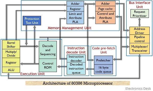
The Intel 80386 marks a significant step forward as a 32-bit microprocessor, introducing features like paging and an enhanced protected mode.
Memory Management and Protection
Memory Management Unit (MMU):
- Adder: Calculates physical addresses from virtual addresses.
- Register Limit and Attribute PLA: Checks segment limits and attributes for memory access.
- Page-cache Control: Manages page caching, enhancing memory access speed.
- Protection Test Unit: Ensures that memory access adheres to the protection rules set by the operating system.
Execution Pipeline and Processing
Execution Unit:
- Barrel Shifter: Offers rapid shifting operations.
- Multiply/Divide Hardware: Dedicated circuits for multiplication and division, speeding up these operations.
- ALU and Register File: Central to arithmetic, logical operations, and data storage.
- Control ROM: Contains microcode for complex instruction execution.
- Decode and Sequencing: Manages instruction decoding and the sequence of execution.
Instruction Processing and Prefetch
Instruction Handling:
- Instruction Decode Unit: Breaks down complex instructions into simpler micro-operations.
- Code Pre-fetch Unit: Anticipates instruction fetch needs.
- 16-byte Code Queue: Ensures a continuous supply of instructions, reducing wait times.
Bus Interface and External Communication
Bus Interface Unit (BIU):
- Request Prioritizer: Manages and prioritizes various bus requests for efficient data transfer.
- Address Driver and Pipeline Control: Controls the flow of addresses and data, optimizing bus usage.
- Multiplexer/Transceiver: Manages the bidirectional data flow between the processor and external devices.
Intel 80486 Architecture
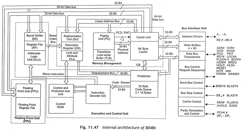
The Intel 80486 processor signifies a leap in integration by combining an on-chip Floating Point Unit (FPU) and cache memory, alongside multiple data buses.
Execution and Processing Units
Core Components:
- Barrel Shifter (BS): Facilitates rapid bit manipulation.
- ALU and Register File (RF): Enhanced for better arithmetic and logical operations, with dedicated registers.
- Integrated FPU: Has its own register file for floating-point operations, increasing computational power.
- Control and Protection Test Unit: Ensures correct operation and enforces security measures.
Memory Management and Caching
Memory System:
- Segmentation Unit (SU) and Paging Unit (PU): Support virtual memory, allowing for large address spaces.
- Translation Lookaside Buffer (TLB): Acts as a cache for memory address translations, speeding up memory access.
- 8KB Cache: On-chip cache reduces memory latency, improving overall performance.
Instruction Processing and Prefetch
Instruction Handling:
- 32-byte Code Queue: Stores instructions ahead of execution, ensuring a constant supply.
- Advanced Instruction Decoder (ID): Breaks down complex instructions for execution.
- Prefetcher: Keeps the code queue filled, minimizing instruction fetch delays.
Bus Interface and System Integration
Bus Management:
- Address Drivers and Write Buffers: Manage address and data output to external systems.
- Data Bus Transceivers: Control data flow between the processor and external devices.
- Bus Control Logic: Divided into specialized sections:
- Bus Control Request Sequencer: Manages bus requests.
- Burst Bus Control: Optimizes bus usage for consecutive data transfers.
- Bus Size Control: Adapts to different data bus widths.
- Cache Control: Manages cache operations.
- Parity Generation and Control: Ensures data integrity.
Intel Pentium Processor Architecture
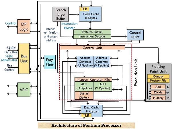
The Intel Pentium processor introduces a dual pipeline design, enhancing performance through superscalar architecture with both 32-bit and 64-bit data paths.
Instruction Processing and Branch Prediction
Instruction Handling:
- 8KB Code Cache: Stores recently used instructions for faster access.
- Branch Target Buffer (BTB): Predicts branch outcomes to reduce execution stalls.
- Branch Verification and Target Address Unit: Fine-tunes branch prediction accuracy and flow.
- Prefetch Buffers: Ensure a continuous supply of instructions to the pipelines.
Execution Units and Register Organization
Execution Core:
- Dual ALUs: Allow for simultaneous execution of integer operations.
- Integrated FPU: Enhances floating-point performance with:
- Dedicated FPU Register File: For floating-point data.
- Specialized Units: For Add, Multiply, and Divide operations.
- Shared Integer Register File: Between the U and V pipelines for efficient data sharing.
Memory Management and Caching
Memory System:
- Page Unit: Supports virtual memory operations.
- Dual TLBs: Separate for code and data, speeding up address translation.
- 8KB Caches (Code and Data): Both utilize a write-back policy to optimize memory usage.
System Interface and Control
Bus and Control:
- Bus Unit: Manages external communication with a 64-bit data bus and a 32-bit address bus.
- Advanced Programmable Interrupt Controller (APIC): Efficiently handles interrupts for multitasking environments.
- Control Unit: Coordinates the operations of the processor’s internal components, ensuring smooth operation across all units.
P6 (Intel Pentium Pro) Processor Architecture
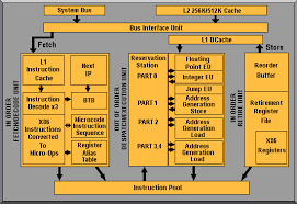
The P6 architecture by Intel is notable for its complex pipeline design, enhancing processor performance through various innovative features.
Instruction Processing and Fetch Unit
Fetch Mechanism:
- Independent Fetch Unit: Fetches instructions from the L2 cache autonomously.
- Branch Prediction: Uses branch prediction and target buffers to speculate on code paths.
- Micro-op Decoding: Instructions are broken down into micro-operations (micro-ops) and placed into an instruction pool for further processing.
Execution Resources and Register Management
Execution Pipeline:
- Multiple Execution Units: Designed for parallel operation, allowing for multiple instructions to be executed simultaneously.
- Register Alias Table (RAT): Manages register renaming, which is crucial for out-of-order execution, preventing false dependencies.
Memory Management and Store Operations
Memory Operations:
- Load and Store Units: Dedicated hardware for managing memory read and write operations.
- Store Buffer: Holds data to be written to memory, optimizing write operations.
- Load Buffer: Manages data reads, supporting speculative execution to accelerate data access.
Retirement and Commitment
Instruction Commitment:
- Retirement Unit: Ensures that instructions are committed to the architectural state in order, despite being executed out-of-order.
- Exception and Interrupt Handling: Manages any exceptions or interrupts, maintaining system integrity.
Intel Pentium III Processor Architecture
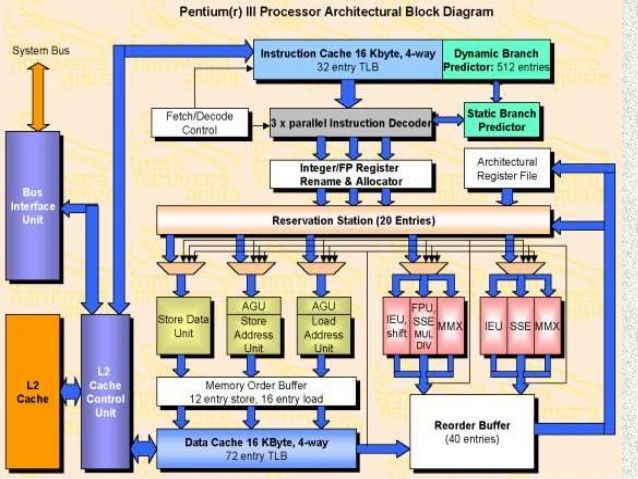
The Pentium III processor builds upon the P6 architecture with several key enhancements:
- Caches: 16 KB instruction cache and 16 KB data cache, both 4-way set associative.
- Instruction Handling: 3x parallel instruction decoder, fetch/decode control, and a 512-entry dynamic branch predictor.
- Out-of-Order Execution: Integer/floating-point register rename and allocator, 20-entry reservation station, and 40-entry reorder buffer.
- Execution Units: AGUs (Address Generation Units), multiple execution units (IEU, FPU) for integer, floating-point, and multimedia instructions.
Intel Pentium 4 Processor Architecture
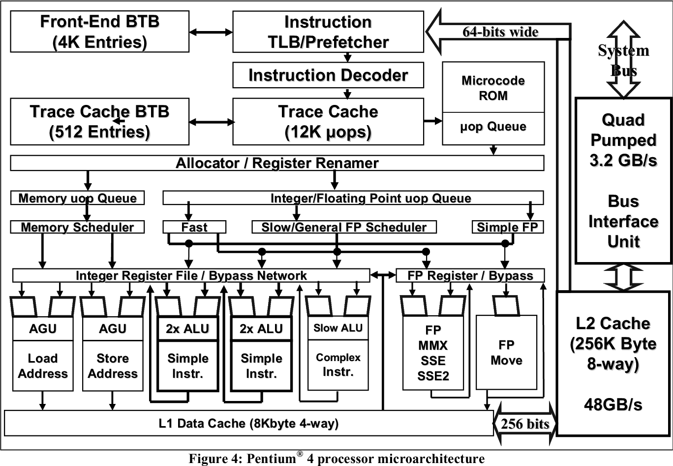
The Pentium 4 processor introduces several advancements in instruction handling and execution efficiency.
Front-End and Instruction Processing
Instruction Fetching:
- 4K-entry Branch Target Buffer (BTB): Improves branch prediction accuracy.
- Instruction TLB/Prefetcher: Uses a 64-bit bus for efficient prefetching of instructions.
- 12K μops Trace Cache: Stores decoded micro-operations (μops), speeding up instruction execution with its own 512-entry Trace Cache BTB.
Instruction Allocation and Scheduling
Resource Management:
- Allocator/Register Renamer: Prepares instructions for execution by renaming registers.
- Specialized Queues:
- Memory μop Queue: For memory-related operations.
- Integer/Floating Point μop Queue: For computational tasks.
- Schedulers:
- Fast Scheduler: For quick, simple instructions.
- Slow/General FP Scheduler: For complex floating-point operations.
- Simple FP Scheduler: For less complex floating-point tasks.
Execution Resources
Execution Units:
- Dedicated AGUs (Address Generation Units): For effective memory address calculations.
- Multiple ALUs: Handle various arithmetic and logical operations.
- Complex Instruction Unit: Manages less frequent but complex instructions.
- Floating-point Hardware: Includes MMX, SSE, and SSE2 units for enhanced multimedia and scientific computing.
- Register/Bypass Networks: Ensure data availability for subsequent instructions.
Memory Hierarchy and System Interface
Cache and Bus:
- 8KB L1 Data Cache: For quick data access.
- 256KB L2 Cache: Larger cache for improved performance.
- Bus Interface Unit: Supports a Quad-Pumped system bus with 3.2 GB/s throughput, while the L2 cache boasts a 48GB/s bandwidth.
Advanced Features and Performance
Performance Enhancements:
- Out-of-Order Execution: Allows instructions to complete in any order for better efficiency.
- Speculative Execution: Predicts and executes instructions speculatively based on branch prediction.
- Sophisticated Branch Prediction: Minimizes delays due to branches in code.
The Pentium 4’s architecture was influential, setting the stage for future processor designs with its emphasis on high-performance computing through advanced instruction processing and execution strategies.